


Please enter the answer below before you can view the full text.
9+1=
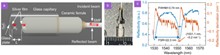
With the rapid development of lithium batteries, it’s of great significance to ensure the safe use of it. An ultrasound imaging system based on fiber optic ultrasound sensor has been developed to monitor the internal changes of lithium batteries. Based on Fabry-Perot interferometer (FPI) structure which is made of a glass plate and an optical fiber pigtail, the ultrasound imaging system possesses a high sensitivity of 558 mV/kPa at 500 kHz with the noise equivalent pressure (NEP) of only 63.5 mPa. For the frequency response, the ultrasound sensitivity is higher than 13.1 mV/kPa within the frequency range from 50 kHz to 1 MHz. Meanwhile, the battery imaging system based on the proposed sensor has a superior resolution as high as 0.5 mm. The performance of battery safety monitoring is verified, in which three commercial lithium-ion ferrous phosphate/graphite (LFP||Gr) batteries are imaged and the state of health (SOH) for different batteries is obtained. Besides, the wetting process of an anode-free lithium metal batteries (AFLMB) is clearly observed via the proposed system, in which the formation process of the pouch cell is analyzed and the gas-related "unwetting" condition is discovered, representing a significant advancement in battery health monitoring field. In the future, the commercial usage can be realized when sensor array and artificial intelligence technology are adopted.
Eco-friendly quantum-dot light-emitting diodes (QLEDs), which employ colloidal quantum dots (QDs) such as InP, and ZnSe, stand out due to their low toxicity, color purity, and high efficiency. Currently, significant advancements have been made in the performance of cadmium-free QLEDs. However, several challenges persist in the industrialization of eco-friendly QLED displays. For instance, (1) the poor performance, characterized by low photoluminescence quantum yield (PLQY), unstable ligand, and charge imbalance, cannot be effectively addressed with a solitary strategy; (2) the degradation mechanism, involving emission quenching, morphological inhomogeneity, and field-enhanced electron delocalization remains unclear; (3) the lack of techniques for color patterning, such as optical lithography and transfer printing. Herein, we undertake a specific review of all technological breakthroughs that endeavor to tackle the above challenges associated with cadmium-free QLED displays. We begin by reviewing the evolution, architecture, and operational characteristics of eco-friendly QLEDs, highlighting the photoelectric properties of QDs, carrier transport layer stability, and device lifetime. Subsequently, we focus our attention not only on the latest insights into device degradation mechanisms, particularly, but also on the remarkable technological progress in color patterning techniques. To conclude, we provide a synthesis of the promising prospects, current challenges, potential solutions, and emerging research trends for QLED displays.
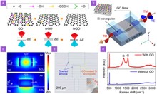
Optical polarizers, which allow the transmission of specific polarization states, are essential components in modern optical systems. Here, we experimentally demonstrate integrated photonic polarizers incorporating reduced graphene oxide (rGO) films. 2D graphene oxide (GO) films are integrated onto silicon waveguides and microring resonators (MRRs) with precise control over their thicknesses and sizes, followed by GO reduction via two different methods including uniform thermal reduction and localized photothermal reduction. We measure devices with various lengths, thicknesses, and reduction degrees of GO films. The results show that the devices with rGO exhibit better performance than those with GO, achieving a polarization-dependent loss of ~47 dB and a polarization extinction ratio of ~16 dB for the hybrid waveguides and MRRs with rGO, respectively. By fitting the experimental results with theory, it is found that rGO exhibits more significant anisotropy in loss, with an anisotropy ratio over 4 times that of GO. In addition, rGO shows higher thermal stability and greater robustness to photothermal reduction than GO. These results highlight the strong potential of rGO films for implementing high-performance polarization selective devices in integrated photonic platforms.
Glucose molecules are of great significance being one of the most important molecules in metabolic chain. However, due to the small Raman scattering cross-section and weak/non-adsorption on bare metals, accurately obtaining their "fingerprint information" remains a huge obstacle. Herein, we developed a tip-enhanced Raman scattering (TERS) technique to address this challenge. Adopting an optical fiber radial vector mode internally illuminates the plasmonic fiber tip to effectively suppress the background noise while generating a strong electric-field enhanced tip hotspot. Furthermore, the tip hotspot approaching the glucose molecules was manipulated via the shear-force feedback to provide more freedom for selecting substrates. Consequently, our TERS technique achieves the visualization of all Raman modes of glucose molecules within spectral window of 400–3200 cm?1, which is not achievable through the far-field/surface-enhanced Raman, or the existing TERS techniques. Our TERS technique offers a powerful tool for accurately identifying Raman scattering of molecules, paving the way for biomolecular analysis.
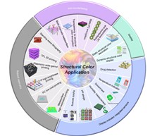
Color as an indispensable element in our life brings vitality to us and enriches our lifestyles through decorations, indicators, and information carriers. Structural color offers an intriguing strategy to achieve novel functions and endows color with additional levels of significance in anti-counterfeiting, display, sensor, and printing. Furthermore, structural colors possess excellent properties, such as resistance to extreme external conditions, high brightness, saturation, and purity. Devices and platforms based on structural color have significantly changed our life and are becoming increasingly important. Here, we reviewed four typical applications of structural color and analyzed their advantages and shortcomings. First, a series of mechanisms and fabrication methods are briefly summarized and compared. Subsequently, recent progress of structural color and its applications were discussed in detail. For each application field, we classified them into several types in terms of their functions and properties. Finally, we analyzed recent emerging technologies and their potential for integration into structural color devices, as well as the corresponding challenges.
With the rapid development of holographic technology, metasurface-based holographic communication schemes have demonstrated immense potential for electromagnetic (EM) multifunctionality. However, traditional passive metasurfaces are severely limited by their lack of reconfigurability, hindering the realization of versatile holographic applications. Origami, an art form that mechanically induces spatial deformations, serves as a platform for multifunctional devices and has garnered significant attention in optics, physics, and materials science. The Miura-ori folding paradigm, characterized by its continuous reconfigurability in folded states, remains unexplored in the context of holographic imaging. Herein, we integrate the principles of Rosenfeld with L- and D-metal chiral enantiomers on a Miura-ori surface to tailor the aperture distribution. Leveraging the continuously tunable nature of the Miura-ori's folded states, the chiral response of the metallic structures varies across different folding configurations, enabling distinct EM holographic imaging functionalities. In the planar state, holographic encryption is achieved. Under specific folding conditions and driven by spin circularly polarized (CP) waves at a particular frequency, multiplexed holographic images can be reconstructed on designated focal planes with CP selectivity. Notably, the fabricated origami metasurface exhibits a large negative Poisson ratio, facilitating portability and deployment and offering novel avenues for spin-selective systems, camouflage, and information encryption.
Diatomic metasurfaces designed for interferometric mechanisms possess significant potential for the multidimensional manipulation of electromagnetic waves, including control over amplitude, phase, frequency, and polarization. Geometric phase profiles with spin-selective properties are commonly associated with wavefront modulation, allowing the implementation of conjugate strategies within orthogonal circularly polarized channels. Simultaneous control of these characteristics in a single-layered diatomic metasurface will be an apparent technological extension. Here, spin-selective modulation of terahertz (THz) beams is realized by assembling a pair of meta-atoms with birefringent effects. The distinct modulation functions arise from geometric phase profiles characterized by multiple rotational properties, which introduce independent parametric factors that elucidate their physical significance. By arranging the key parameters, the proposed design strategy can be employed to realize independent amplitude and phase manipulation. A series of THz metasurface samples with specific modulation functions are characterized, experimentally demonstrating the accuracy of on-demand manipulation. This research paves the way for all-silicon meta-optics that may have great potential in imaging, sensing and detection.
Structured illumination, a wide-field imaging approach used in microscopy to enhance image resolution beyond the system's diffraction limits, is a well-studied technique that has gained significant traction over the last two decades. However, when translated to endoscopic systems, severe deformations of illumination patterns occur due to the large depth of field (DOF) and the 3D nature of the targets, introducing significant implementation challenges. Hence, this study explores a speckle-based system that best suits endoscopic practices to enhance image resolution by using random illumination patterns. The study presents a prototypic model of an endoscopic add-on, its design, and fabrication facilitated by using the speckle structured illumination endoscopic (SSIE) system. The imaging results of the SSIE are explained on a colon phantom model at different imaging planes with a wide field of view (FOV) and DOF. The obtained imaging metrics are elucidated and compared with state-of-the-art (SOA) high-resolution endoscopic techniques. Moreover, the potential for a clinical translation of the prototypic SSIE model is also explored in this work. The incorporation of the add-on and its subsequent results on the colon phantom model could potentially pave the way for its successful integration and use in futuristic clinical endoscopic trials.
On-chip devices for generating pre-designed vectorial optical fields (VOFs) under surface wave (SW) excitations are highly desired in integrated photonics. However, conventional devices are usually of large footprints, low efficiencies, and limited wave-control capabilities. Here, we present a generic approach to design ultra-compact on-chip devices that can efficiently generate pre-designed VOFs under SW excitations, and experimentally verify the concept in terahertz (THz) regime. We first describe how to design SW-excitation metasurfaces for generating circularly polarized complex beams, and experimentally demonstrate two meta-devices to realize directional emission and focusing of THz waves with opposite circular polarizations, respectively. We then establish a systematic approach to construct an integrated device via merging two carefully designed metasurfaces, which, under SW excitations, can separately produce pre-designed far-field patterns with different circular polarizations and generate target VOF based on their interference. As a proof of concept, we demonstrate experimentally a meta-device that can generate a radially polarized Bessel beam under SW excitation at ~0.4 THz. Experimental results agree well with full-wave simulations, collectively verifying the performance of our device. Our study paves the road to realizing highly integrated on-chip functional THz devices, which may find many applications in biological sensing, communications, displays, image multiplexing, and beyond.
This work introduces special states for light in multimode fibers featuring strongly enhanced or reduced correlations between output fields in the presence of environmental temperature fluctuations. Using experimentally measured multi-temperature transmission matrix, a set of temperature principal modes that exhibit resilience to disturbances caused by temperature fluctuations can be generated. Reversing this concept also allows the construction of temperature anti-principal modes, with output profiles more susceptible to temperature influences than the unmodulated wavefront. Despite changes in the length of the multimode fiber within the temperature-fluctuating region, the proposed approach remains capable of robustly controlling the temperature response within the fiber. To illustrate the practicality of the proposed special state, a learning-empowered fiber specklegram temperature sensor based on temperature anti-principal mode sensitization is proposed. This sensor exhibits outstanding superiority over traditional approaches in terms of resolution and accuracy. These novel states are anticipated to have wide-ranging applications in fiber communication, sensing, imaging, and spectroscopy, and serve as a source of inspiration for the discovery of other novel states.
Metasurfaces, composed of planar arrays of intricately designed meta-atom structures, possess remarkable capabilities in controlling electromagnetic waves in various ways. A critical aspect of metasurface design involves selecting suitable meta-atoms to achieve target functionalities such as phase retardation, amplitude modulation, and polarization conversion. Conventional design processes often involve extensive parameter sweeping, a laborious and computationally intensive task heavily reliant on designer expertise and judgement. Here, we present an efficient genetic algorithm assisted meta-atom optimization method for high-performance metasurface optics, which is compatible to both single- and multi-objective device design tasks. We first employ the method for a single-objective design task and implement a high-efficiency Pancharatnam-Berry phase based metalens with an average focusing efficiency exceeding 80% in the visible spectrum. We then employ the method for a dual-objective metasurface design task and construct an efficient spin-multiplexed structural beam generator. The device is capable of generating zeroth-order and first-order Bessel beams respectively under right-handed and left-handed circular polarized illumination, with associated generation efficiencies surpassing 88%. Finally, we implement a wavelength and spin co-multiplexed four-channel metahologram capable of projecting two spin-multiplexed holographic images under each operational wavelength, with efficiencies over 50%. Our work offers a streamlined and easy-to-implement approach to meta-atom design and optimization, empowering designers to create diverse high-performance and multifunctional metasurface optics.
The increasing popularity of the metaverse has led to a growing interest and market size in spatial computing from both academia and industry. Developing portable and accurate imaging and depth sensing systems is crucial for advancing next-generation virtual reality devices. This work demonstrates an intelligent, lightweight, and compact edge-enhanced depth perception system that utilizes a binocular meta-lens for spatial computing. The miniaturized system comprises a binocular meta-lens, a 532 nm filter, and a CMOS sensor. For disparity computation, we propose a stereo-matching neural network with a novel H-Module. The H-Module incorporates an attention mechanism into the Siamese network. The symmetric architecture, with cross-pixel interaction and cross-view interaction, enables a more comprehensive analysis of contextual information in stereo images. Based on spatial intensity discontinuity, the edge enhancement eliminates ill-posed regions in the image where ambiguous depth predictions may occur due to a lack of texture. With the assistance of deep learning, our edge-enhanced system provides prompt responses in less than 0.15 seconds. This edge-enhanced depth perception meta-lens imaging system will significantly contribute to accurate 3D scene modeling, machine vision, autonomous driving, and robotics development.
Photonic signal processing offers a versatile and promising toolkit for contemporary scenarios ranging from digital optical communication to analog microwave operation. Compared to its electronic counterpart, it eliminates inherent bandwidth limitations and meanwhile exhibits the potential to provide unparalleled scalability and flexibility, particularly through integrated photonics. However, by far the on-chip solutions for optical signal processing are often tailored to specific tasks, which lacks versatility across diverse applications. Here, we propose a streamlined chip-level signal processing architecture that integrates different active and passive building blocks in silicon-on-insulator (SOI) platform with a compact and efficient manner. Comprehensive and in-depth analyses for the architecture are conducted at levels of device, system, and application. Accompanied by appropriate configuring schemes, the photonic circuitry supports loading and processing both analog and digital signals simultaneously. Three distinct tasks are facilitated with one single chip across several mainstream fields, spanning optical computing, microwave photonics, and optical communications. Notably, it has demonstrated competitive performance in functions like image processing, spectrum filtering, and electro-optical bandwidth equalization. Boasting high universality and a compact form factor, the proposed architecture is poised to be instrumental for next-generation functional fusion systems.
As a combination of fiber optics and nanotechnology, optical micro/nanofiber (MNF) is considered as an important multifunctional building block for fabricating various miniaturized photonic devices. With the rapid progress in flexible opto-electronics, MNF has been emerging as a promising candidate for assembling tactile sensors and soft actuators owing to its unique optical and mechanical properties. This review discusses the advances in MNF enabled tactile sensors and soft actuators, specifically, focusing on the latest research results over the past 5 years and the applications in health monitoring, human-machine interfaces, and robotics. Future prospects and challenges in developing flexible MNF devices are also presented.
Light–matter interactions in two-dimensional (2D) materials have been the focus of research since the discovery of graphene. The light–matter interaction length in 2D materials is, however, much shorter than that in bulk materials owing to the atomic nature of 2D materials. Plasmonic nanostructures are usually integrated with 2D materials to enhance the light–matter interactions, offering great opportunities for both fundamental research and technological applications. Nanoparticle-on-mirror (NPoM) structures with extremely confined optical fields are highly desired in this aspect. In addition, 2D materials provide a good platform for the study of plasmonic fields with subnanometer resolution and quantum plasmonics down to the characteristic length scale of a single atom. A focused and up-to-date review article is highly desired for a timely summary of the progress in this rapidly growing field and to encourage more research efforts in this direction. In this review, we will first introduce the basic concepts of plasmonic modes in NPoM structures. Interactions between plasmons and quasi-particles in 2D materials, e.g., excitons and phonons, from weak to strong coupling and potential applications will then be described in detail. Related phenomena in subnanometer metallic gaps separated by 2D materials, such as quantum tunneling, will also be touched. We will finally discuss phenomena and physical processes that have not been understood clearly and provide an outlook for future research. We believe that the hybrid systems of 2D materials and NPoM structures will be a promising research field in the future.
This paper presents a wide-bandwidth back-illuminated modified uni-traveling-carrier photodiode (MUTC-PD) packaged with standard WR-5 rectangular waveguide for high-speed wireless communications. With optimized epitaxy structure and coplanar waveguide electrodes, the fabricated 4-μm-diameter PD exhibits ultra-flat frequency response and high saturation power. Integrated passive circuits including low-loss bias-tee and E-plane probe are designed to package the PD into a compact module with waveguide output. The packaged PD module has demonstrated a flat frequency response with fluctuations within ±2.75 dB over a broadband of 140–220 GHz and a high saturated output power of ?7.8 dBm (166 μW) at 140 GHz. For wireless communication applications, the packaged PD is used to implement 1-m free space transmission at carrier frequencies of 150.5 and 210.5 GHz, with transmission rates of 75 and 90 Gbps, respectively.
Phonon polaritons (PhPs) exhibit directional in-plane propagation and ultralow losses in van der Waals (vdW) crystals, offering new possibilities for controlling the flow of light at the nanoscale. However, these PhPs, including their directional propagation, are inherently determined by the anisotropic crystal structure of the host materials. Although in-plane anisotropic PhPs can be manipulated by twisting engineering, such as twisting individual vdW slabs, dynamically adjusting their propagation presents a significant challenge. The limited application of the twisted bilayer structure in bare films further restricts its usage. In this study, we present a technique in which anisotropic PhPs supported by bare biaxial vdW slabs can be actively tuned by modifying their local dielectric environment. Excitingly, we predict that the iso-frequency contour of PhPs can be reoriented to enable propagation along forbidden directions when the crystal is placed on a substrate with a moderate negative permittivity. Besides, we systematically investigate the impact of polaritonic coupling on near-field radiative heat transfer (NFRHT) between heterostructures integrated with different substrates that have negative permittivity. Our main findings reveal that through the analysis of dispersion contour and photon transmission coefficient, the excitation and reorientation of the fundamental mode facilitate increased photon tunneling, thereby enhancing heat transfer between heterostructures. Conversely, the annihilation of the fundamental mode hinders heat transfer. Furthermore, we find the enhancement or suppression of radiative energy transport depends on the relative magnitude of the slab thickness and the vacuum gap width. Finally, the effect of negative permittivity substrates on NFRHT along the [001] crystalline direction of α-MoO3 is considered. The spectral band where the excited fundamental mode resulting from the negative permittivity substrates is shifted to the first Reststrahlen Band (RB 1) of α-MoO3 and is widened, resulting in more significant enhancement of heat flux from RB 1. We anticipate our results will motivate new direction for dynamical tunability of the PhPs in photonic devices.
GHz burst-mode femtosecond (fs) laser, which emits a series of pulse trains with extremely short intervals of several hundred picoseconds, provides distinct characteristics in materials processing as compared with the conventional irradiation scheme of fs laser (single-pulse mode). In this paper, we take advantage of the moderate pulse interval of 205 ps (4.88 GHz) in the burst pulse for high-quality and high-efficiency micromachining of single crystalline sapphire by laser induced plasma assisted ablation (LIPAA). Specifically, the preceding pulses in the burst generate plasma by ablation of copper placed behind the sapphire substrate, which interacts with the subsequent pulses to induce ablation at the rear surface of sapphire substrates. As a result, not only the ablation quality but also the ablation efficiency and the fabrication resolution are greatly improved compared to the other schemes including single-pulse mode fs laser direct ablation, single-pulse mode fs-LIPAA, and nanosecond-LIPAA.
Conventionally, the spatially structured light beams produced by metasurfaces primarily highlight the polarization modulation of the beams propagating along the optical axis or the beams' spatial transmission trajectory. In particular, along the optical axis, the polarization state is either constant or varies continuously in each output plane. Here, we develop innovative spatially structured light beams with continually changing polarization along any arbitrary spatial transmission trajectories. With tri-layer metallic metasurfaces, the geometric characteristics of each layer structure can be adjusted to modulate the phase and polarization state of the incident terahertz (THz) wave. The beam will converge to the predefined trajectory along several paths to generate a Bessel-like beam with longitudinal polarization changes. We demonstrate the versatility of the approach by designing two THz-band structured light beams with varying polarization states along the spatial helical transmission trajectory. Continuous linear polarization changes and linear polarization to right circular polarization (RCP) and back to linear polarization changes are realized respectively. The experimental results are basically consistent with the simulated results. Our proposal for arbitrary trajectory structured light beams with longitudinally varying polarization offers a practical method for continuously regulating the characteristics of spatial structured light beams with non-axial transmission. This technique has potential uses in optical encryption, particle manipulation, and biomedical imaging.
The integration between infrared detection and modern microelectronics offers unique opportunities for compact and high-resolution infrared imaging. However, silicon, the cornerstone of modern microelectronics, can only detect light within a limited wavelength range (< 1100 nm) due to its bandgap of 1.12 eV, which restricts its utility in the infrared detection realm. Herein, a photo-driven fin field-effect transistor is presented, which breaks the spectral response constraint of conventional silicon detectors while achieving sensitive infrared detection. This device comprises a fin-shaped silicon channel for charge transport and a lead sulfide film for infrared light harvesting. The lead sulfide film wraps the silicon channel to form a “three-dimensional” infrared-sensitive gate, enabling the photovoltage generated at the lead sulfide-silicon junction to effectively modulate the channel conductance. At room temperature, this device realizes a broadband photodetection from visible (635 nm) to short-wave infrared regions (2700 nm), surpassing the working range of the regular indium gallium arsenide and germanium detectors. Furthermore, it exhibits low equivalent noise powers of 3.2×10?12 W·Hz?1/2 and 2.3×10?11 W·Hz?1/2 under 1550 nm and 2700 nm illumination, respectively. These results highlight the significant potential of photo-driven fin field-effect transistors in advancing uncooled silicon-based infrared detection.
Integrated photonic devices are essential for on-chip optical communication, optical-electronic systems, and quantum information sciences. To develop a high-fidelity interface between photonics in various frequency domains without disturbing their quantum properties, nonlinear frequency conversion, typically steered with the quadratic (χ2) process, should be considered. Furthermore, another degree of freedom in steering the spatial modes during the χ2 process, with unprecedent mode intensity is proposed here by modulating the lithium niobate (LN) waveguide-based inter-mode quasi-phase-matching conditions with both temperature and wavelength parameters. Under high incident light intensities (25 and 27.8 dBm for the pump and the signal lights, respectively), mode conversion at the sum-frequency wavelength with sufficient high output power (?7 – 8 dBm) among the TM01, TM10, and TM00 modes is realized automatically with characterized broad temperature (ΔT ≥ 8 °C) and wavelength windows (Δλ ≥ 1 nm), avoiding the previous efforts in carefully preparing the signal or pump modes. The results prove that high-intensity spatial modes can be prepared at arbitrary transparent wavelength of the χ2 media toward on-chip integration, which facilitates the development of chip-based communication and quantum information systems because spatial correlations can be applied to generate hyperentangled states and provide additional robustness in quantum error correction with the extended Hilbert space.
Quantum dot-based up-conversion photodetector, in which an infrared photodiode (PD) and a quantum dot light-emitting diode (QLED) are back-to-back connected, is a promising candidate for low-cost infrared imaging. However, the huge efficiency losses caused by integrating the PD and QLED together hasn’t been studied sufficiently. This work revealed at least three origins for the efficiency losses. First, the PD unit and QLED unit usually didn’t work under optimal conditions at the same time. Second, the potential barriers and traps at the interconnection between PD and QLED units induced unfavorable carrier recombination. Third, much emitted visible light was lost due to the strong visible absorption in the PD unit. Based on the understandings on the loss mechanisms, the infrared up-conversion photodetectors were optimized and achieved a breakthrough photon-to-photon conversion efficiency of 6.9%. This study provided valuable guidance on how to optimize the way of integration for up-conversion photodetectors.
Optical endoscopy has become an essential diagnostic and therapeutic approach in modern biomedicine for directly observing organs and tissues deep inside the human body, enabling non-invasive, rapid diagnosis and treatment. Optical fiber endoscopy is highly competitive among various endoscopic imaging techniques due to its high flexibility, compact structure, excellent resolution, and resistance to electromagnetic interference. Over the past decade, endoscopes based on a single multimode optical fiber (MMF) have attracted widespread research interest due to their potential to significantly reduce the footprint of optical fiber endoscopes and enhance imaging capabilities. In comparison with other imaging principles of MMF endoscopes, the scanning imaging method based on the wavefront shaping technique is highly developed and provides benefits including excellent imaging contrast, broad applicability to complex imaging scenarios, and good compatibility with various well-established scanning imaging modalities. In this review, various technical routes to achieve light focusing through MMF and procedures to conduct the scanning imaging of MMF endoscopes are introduced. The advancements in imaging performance enhancements, integrations of various imaging modalities with MMF scanning endoscopes, and applications are summarized. Challenges specific to this endoscopic imaging technology are analyzed, and potential remedies and avenues for future developments are discussed.
Femtosecond laser-induced periodic surface structures (LIPSS) have been extensively studied over the past few decades. In particular, the period and groove width of high-spatial-frequency LIPSS (HSFL) is much smaller than the diffraction limit, making it a useful method for efficient nanomanufacturing. However, compared with the low-spatial-frequency LIPSS (LSFL), the structure size of the HSFL is smaller, and it is more easily submerged. Therefore, the formation mechanism of HSFL is complex and has always been a research hotspot in this field. In this study, regular LSFL with a period of 760 nm was fabricated in advance on a silicon surface with two-beam interference using an 800 nm, 50 fs femtosecond laser. The ultrafast dynamics of HSFL formation on the silicon surface of prefabricated LSFL under single femtosecond laser pulse irradiation were observed and analyzed for the first time using collinear pump-probe imaging method. In general, the evolution of the surface structure undergoes five sequential stages: the LSFL begins to split, becomes uniform HSFL, degenerates into an irregular LSFL, undergoes secondary splitting into a weakly uniform HSFL, and evolves into an irregular LSFL or is submerged. The results indicate that the local enhancement of the submerged nanocavity, or the nanoplasma, in the prefabricated LSFL ridge led to the splitting of the LSFL, and the thermodynamic effect drove the homogenization of the splitting LSFL, which evolved into HSFL.
This study reviews the recent advances in data-driven polarimetric imaging technologies based on a wide range of practical applications. The widespread international research and activity in polarimetric imaging techniques demonstrate their broad applications and interest. Polarization information is increasingly incorporated into convolutional neural networks (CNN) as a supplemental feature of objects to improve performance in computer vision task applications. Polarimetric imaging and deep learning can extract abundant information to address various challenges. Therefore, this article briefly reviews recent developments in data-driven polarimetric imaging, including polarimetric descattering, 3D imaging, reflection removal, target detection, and biomedical imaging. Furthermore, we synthetically analyze the input, datasets, and loss functions and list the existing datasets and loss functions with an evaluation of their advantages and disadvantages. We also highlight the significance of data-driven polarimetric imaging in future research and development.
Simultaneously manipulating multiple physical fields plays an important role in the increasingly complex integrated systems, aerospace equipment, biochemical productions, etc. For on-chip systems with high integration level, the precise and efficient control of the propagation of electromagnetic waves and heat fluxes simultaneously is particularly important. In this study, we propose a graphical designing method (i.e., thermal-electromagnetic surface transformation) based on thermal-electromagnetic null medium to simultaneously control the propagation of electromagnetic waves and thermal fields according to the pre-designed paths. A thermal-electromagnetic cloak, which can create a cloaking effect on both electromagnetic waves and thermal fields simultaneously, is designed by thermal-electromagnetic surface transformation and verified by both numerical simulations and experimental measurements. The thermal-electromagnetic surface transformation proposed in this study provides a new methodology for simultaneous controlling on electromagnetic and temperature fields, and may have significant applications in improving thermal-electromagnetic compatibility problem, protecting of thermal-electromagnetic sensitive components, and improving efficiency of energy usage for complex on-chip systems.
Real-time acquisition of human pulse signals in daily life is clinically important for cardiovascular disease monitoring and diagnosis. Here, we propose a smart photonic wristband for pulse signal monitoring based on speckle pattern analysis with a polymer optical fiber (POF) integrated into a sports wristband. Several different speckle pattern processing algorithms and POFs with different core diameters were evaluated. The results indicated that the smart photonic wristband had a high signal-to-noise ratio and low latency, with the measurement error controlled at approximately 3.7%. This optimized pulse signal could be used for further medical diagnosis and was capable of objectively monitoring subtle pulse signal changes, such as the pulse waveform at different positions of Cunkou and pulse waveforms before and after exercise. With the assistance of artificial intelligence (AI), functions such as gesture recognition have been realized through the established prediction model by processing pulse signals, in which the recognition accuracy reaches 95%. Our AI-assisted smart photonic wristband has potential applications for clinical treatment of cardiovascular diseases and home monitoring, paving the way for medical Internet of Things-enabled smart systems.
Distributed fiber gratings exhibit outstanding capabilities in achieving a wide spectral response through the superimposition of gratings with different periods in the fiber core. This significantly broadens the design flexibility and potential applications of fiber gratings. However, as photons pass through gratings with varying periods in sequence, which not only inevitably existing signal crosstalk but also poses challenges for integrating. In this study, a three-dimensional (3D) four-channel filter is proposed and realized in fiber-compatible materials using femtosecond laser writing. The filter consists of a 3D beam splitter and four parallel different-period Bragg waveguide gratings (WGs). By designing grating periods in each path, parallel filtering and reflection at multiple designed wavelengths are achieved compactly with 50 nm spectrum spacing within 1450–1600 nm wavelengths. The four-channel filter entire measures 15.5 mm × 1 mm × 1 mm (the highest integration of distributed fiber gratings reported so far). Our technique will augment the laser fabrication technology for 3D integrated photonic devices and serve as a powerful and generalized solution for highly integrated in-situ measurement and multi-parameter decoupled sensing.
In this paper, a novel highly sensitive methane (CH4) and acetylene (C2H2) dual-gas light-induced thermoelectric spectroscopy (LITES) sensor based on Lissajous space-division multiplexed (LSDM) technology and trapezoidal-head quartz tuning fork (QTF) detector was reported for the first time. A theoretical LSDM model was established on the basis of three-mirror astigmatic multi-pass cell (MPC) and it was used to design a pair of Lissajous spot patterns with optical path length to volume ratios (OPL/Vs) of 13.5 cm?2 and 13.3 cm?2, respectively. Two self-designed trapezoidal-head QTFs with low resonant frequencies of less than 10 kHz and quality factor of ~12000 were adopted to enhance the detection ability. Two kinds of fiber amplifier, erbium doped fiber amplifier (EDFA) and Raman fiber amplifier (RFA), were combined to amplify the output power of two diode lasers to improve the excitation strength. After optimization, minimum detection limit (MDL) of 268.8 ppb and 91.4 ppb for real-simultaneous CH4 and C2H2 sensing were obtained, respectively. When the integration time of the system were 150 s and 100 s, the MDLs could be improved to 54.8 ppb and 26.1 ppb, accordingly. Further improvement methods for such sensor were discussed.
One dimensional sub-wavelength gratings, also known as metagratings have attracted enormous attention due to the relatively simpler design configurations with versatile application potentials. In recent times, these metagratings have played crucial roles in terahertz frequency domain to realize several fascinating effects. It has been demonstrated that the terahertz characteristics of these metagratings can be modified by carefully designing the grating geometry along with meticulously tuning the material characteristics. Such variations in grating design have led to enhanced device performances. In addition, suitably designed metagratings are capable of exciting strong evanescent orders that can be exploited in ultrasensitive sensing, optical trapping, non-linearity, etc. Based on the tremendous potentials offered by the planar geometry (ease of fabrication) along with diverse utilities, we have reviewed few representative works pertaining to terahertz metagratings in this article. Hence, we have discussed metagratings based antireflection coating and a polarization beam splitter operating in THz region modelled using simplified model method. Further, we have discussed experimental detection of evanescent waves excited in metagratings utilizing Fourier transformed terahertz spectroscopy (FTTS) technique. FTTS is a unique technique because of its ability of simultaneous detection of propagating and non-propagating orders. Next, we have discussed applications of metagratings in sensing trace amount of analytes. Considering the increasing interests in these one-dimensional artificial subwavelength structures, we believe, our article will be useful for the researchers willing to begin work on terahertz subwavelength gratings.
Multidimensional-engineering chalcogenide glasses is widely explored to construct various infrared photonic devices, with their surface as a key dimension for wavefront control. Here, we demonstrate direct patterning high-aspect-ratio microstructures on the surface of chalcogenide glasses offers an efficient and robust method to manipulate longwave infrared radiations. Despite chalcogenide glass being considered soft in terms of its mechanical properties, we successfullyfabricate high-aspect-ratio micropillars with a height of 8 μm using optimized deep etching process, and we demonstrate a 2-mm-diameter all-chalcogenide metalens with a numerical aperture of 0.45 on the surface of a 1.5-mm-thick As2Se3 glass. Leveraging the exceptional longwave infrared (LWIR) transparency and moderate refractive index of As2Se3 glass, the all-chalcogenide metalens produces a focal spot size of ~1.39λ0 with a focusing efficiency of 47% at the wavelength of 9.78 μm, while also exhibiting high-resolution imaging capabilities. Our work provides a promising route to realize easy-to-fabricate, mass-producible planar infrared optics for compact, light-weight LWIR imaging systems.
Design of multiple-feed lens antennas requires multivariate and multi-objective optimization processes, which can be accelerated by PSO algorithms. However, the PSO algorithm often fails to achieve optimal results with limited computation resources since spaces of candidate solutions are quite large for lens antenna designs. This paper presents a design paradigm for multiple-feed lens antennas based on a physics-assisted particle swarm optimization (PA-PSO) algorithm, which guides the swarm of particles based on laws of physics. As a proof of concept, a design of compact metalens antenna is proposed, which measures unprecedented performances, such as a field of view at ±55°, a 21.7 dBi gain with a flatness within 4 dB, a 3-dB bandwidth >12°, and a compact design with a f-number of 0.2. The proposed PA-PSO algorithm reaches the optimal results 6 times faster than the ordinary PSO algorithm, which endows promising applications in the multivariate and multi-objective optimization processes, including but not limited to metalens antenna designs.
Supercritical lens (SCL) can break the diffraction limit in the far field and has been demonstrated for high-resolution scanning confocal imaging. Its capability in sharper focusing and needle-like long focal depth should allow high-resolution lithography at violet or ultraviolet (UV) wavelength, however, this has never been experimentally demonstrated. As a proof of concept, in this paper SCLs operating at 405 nm (h-line) wavelength with smaller full-width-at-half-maximum focal spot and longer depth of focus than conventional Fresnel zone lens while maintaining controlled side lobes are designed for direct laser writing (DLW) lithography. Aluminum nitride (AlN) with a high refractive index and low loss in UV-visible range is used to fabricate nanopillar-based metasurfaces structure for the metalens. Grating arrays with improved pitch resolution are fabricated using the SCLs with sub-diffraction-limit focusing capability. The AlN-based metasurface for SCLs at short wavelength for DLW could extend further to UV or deep UV lithography and might be of great interest to both the research and industry applications.
The ability to overcome the negative effects, induced by obstacles and turbulent atmosphere, is a core challenge of long-distance information transmission, and it is of great significance in free-space optical communication. The spatial-coherence structure, that characterizes partially coherent fields, provides a new degree of freedom for carrying information. However, due to the influence of the complex transmission environment, the spatial-coherence structure is severely damaged during the propagation path, which undoubtedly limits its ability to transmit information. Here, we realize the robust far-field orbital angular momentum (OAM) transmission and detection by modulating the spatial-coherence structure of a partially coherent vortex beam with the help of the cross-phase. The cross-phase enables the OAM information, quantified by the topological charge, hidden in the spatial-coherence structure can be stably transmitted to the far field and can resist the influence of obstructions and turbulence within the communication link. This is due to the self-reconstruction property of the spatial-coherence structure embedded with the cross-phase. We demonstrate experimentally that the topological charge information can be recognized well by measuring the spatial-coherence structure in the far field, exhibiting a set of distinct and separated dark rings even under amplitude and phase perturbations. Our findings open a door for robust optical signal transmission through the complex environment and may find application in optical communication through a turbulent atmosphere.
Deconvolution is a commonly employed technique for enhancing image quality in optical imaging methods. Unfortunately, its application in optical coherence tomography (OCT) is often hindered by sensitivity to noise, which leads to additive ringing artifacts. These artifacts considerably degrade the quality of deconvolved images, thereby limiting its effectiveness in OCT imaging. In this study, we propose a framework that integrates numerical random phase masks into the deconvolution process, effectively eliminating these artifacts and enhancing image clarity. The optimized joint operation of an iterative Richardson-Lucy deconvolution and numerical synthesis of random phase masks (RPM), termed as Deconv-RPM, enables a 2.5-fold reduction in full width at half-maximum (FWHM). We demonstrate that the Deconv-RPM method significantly enhances image clarity, allowing for the discernment of previously unresolved cellular-level details in nonkeratinized epithelial cells exvivo and moving blood cells invivo.
Spiking neural networks (SNNs) utilize brain-like spatiotemporal spike encoding for simulating brain functions. Photonic SNN offers an ultrahigh speed and power efficiency platform for implementing high-performance neuromorphic computing. Here, we proposed a multi-synaptic photonic SNN, combining the modified remote supervised learning with delay-weight co-training to achieve pattern classification. The impact of multi-synaptic connections and the robustness of the network were investigated through numerical simulations. In addition, the collaborative computing of algorithm and hardware was demonstrated based on a fabricated integrated distributed feedback laser with a saturable absorber (DFB-SA), where 10 different noisy digital patterns were successfully classified. A functional photonic SNN that far exceeds the scale limit of hardware integration was achieved based on time-division multiplexing, demonstrating the capability of hardware-algorithm co-computation.
Optical nanoparticles are nowadays one of the key elements of photonics. They do not only allow optical imaging of a plethora of systems (from cells to microelectronics), but, in many cases, they also behave as highly sensitive remote sensors. In recent years, it has been demonstrated the success of optical tweezers in isolating and manipulating individual optical nanoparticles. This has opened the door to high resolution single particle scanning and sensing. In this quickly growing field, it is now necessary to sum up what has been achieved so far to identify the appropriate system and experimental set-up required for each application. In this review article we summarize the most relevant results in the field of optical trapping of individual optical nanoparticles. After systematic bibliographic research, we identify the main families of optical nanoparticles in which optical trapping has been demonstrated. For each case, the main advances and applications have been described. Finally, we also include our critical opinion about the future of the field, identifying the challenges that we are facing.
Spatial light modulators, as dynamic flat-panel optical devices, have witnessed rapid development over the past two decades, concomitant with the advancements in micro- and opto-electronic integration technology. In particular, liquid-crystal spatial light modulator (LC-SLM) technologies have been regarded as versatile tools for generating arbitrary optical fields and tailoring all degrees of freedom beyond just phase and amplitude. These devices have gained significant interest in the nascent field of structured light in space and time, facilitated by their ease of use and real-time light manipulation, fueling both fundamental research and practical applications. Here we provide an overview of the key working principles of LC-SLMs and review the significant progress made to date in their deployment for various applications, covering topics as diverse as beam shaping and steering, holography, optical trapping and tweezers, measurement, wavefront coding, optical vortex, and quantum optics. Finally, we conclude with an outlook on the potential opportunities and technical challenges in this rapidly developing field.
Virtual reality (VR) and augmented reality (AR) are revolutionizing our lives. Near-eye displays are crucial technologies for VR and AR. Despite the rapid advances in near-eye display technologies, there are still challenges such as large field of view, high resolution, high image quality, natural free 3D effect, and compact form factor. Great efforts have been devoted to striking a balance between visual performance and device compactness. While traditional optics are nearing their limitations in addressing these challenges, ultra-thin metasurface optics, with their high light-modulating capabilities, may present a promising solution. In this review, we first introduce VR and AR near-eye displays, and then briefly explain the working principles of light-modulating metasurfaces, review recent developments in metasurface devices geared toward near-eye display applications, delved into several advanced natural 3D near-eye display technologies based on metasurfaces, and finally discuss about the remaining challenges and future perspectives associated with metasurfaces for near-eye display applications.
Hall effect of light is a result of symmetry breaking in spin and/or orbital angular momentum (OAM) possessing optical system and is caused by e.g. refractive index gradient/interface between media or focusing of a spatially asymmetrical beam, similar to the electric field breaking the symmetry in spin Hall effect for electrons. The angular momentum (AM) conservation law in the ensuing asymmetric system dictates redistribution of spin and orbital angular momentum, and is manifested in spin-orbit, orbit-orbit, and orbit-spin conversions and reorganization, i.e. spin-orbit and orbit-orbit interaction. This AM restructuring in turn requires shifts of the barycenter of the electric field of light. In the present study we show, both analytically and by numerical simulation, how different electric field components are displaced upon tight focusing of an asymmetric light beam having OAM and spin. The relation between field components shifts and the AM components shifts/redistribution is presented too. Moreover, we experimentally demonstrate, for the first time, to the best of our knowledge, the spin-orbit Hall effect of light upon tight focusing in free space. This is achieved using azopolymers as a media detecting longitudinal or z component of the electrical field of light. These findings elucidate the Hall effect of light and may broaden the spectrum of its applications.
Graphene and related two-dimensional materials have attracted great research interests due to prominently optical and electrical properties and flexibility in integration with versatile photonic structures. Here, we report an in-fiber photoelectric device by wrapping a few-layer graphene and bonding a pair of electrodes onto a tilted fiber Bragg grating (TFBG) for photoelectric and electric-induced thermo-optic conversions. The transmitted spectrum from this device consists of a dense comb of narrowband resonances that provides an observable window to sense the photocurrent and the electrical injection in the graphene layer. The device has a wavelength-sensitive photoresponse with responsivity up to 11.4 A/W, allowing the spectrum analysis by real-time monitoring of photocurrent evolution. Based on the thermal-optic effect of electrical injection, the graphene layer is energized to produce a global red-shift of the transmission spectrum of the TFBG, with a high sensitivity approaching 2.167×10⁴ nm/A2. The in-fiber photoelectric device, therefore as a powerful tool, could be widely available as off-the-shelf product for photodetection, spectrometer and current sensor.
Energy harvesting plays a crucial role in modern society. In the past years, solar energy, owing to its renewable, green, and infinite attributes, has attracted increasing attention across a broad range of applications from small-scale wearable electronics to large-scale energy powering. However, the utility of solar cells in providing a stable power supply for various electrical appliances in practical applications is restricted by weather conditions. To address this issue, researchers have made many efforts to integrate solar cells with other types of energy harvesters, thus developing hybrid energy harvesters (HEHs), which can harvest energy from the ambient environment via different working mechanisms. In this review, four categories of energy harvesters including solar cells, triboelectric nanogenerators (TENGs), piezoelectric nanogenerators (PENGs), and thermoelectric generators (TEGs) are introduced. In addition, we systematically summarize the recent progress in solar cell-based hybrid energy harvesters (SCHEHs) with a focus on their structure designs and the corresponding applications. Three hybridization designs through unique combinations of TENG, PENG, and TEG with solar cells are elaborated in detail. Finally, the main challenges and perspectives for the future development of SCHEHs are discussed.
Although the 5G wireless network has made significant advances, it is not enough to accommodate the rapidly rising requirement for broader bandwidth in post-5G and 6G eras. As a result, emerging technologies in higher frequencies including visible light communication (VLC), are becoming a hot topic. In particular, LED-based VLC is foreseen as a key enabler for achieving data rates at the Tb/s level in indoor scenarios using multi-color LED arrays with wavelength division multiplexing (WDM) technology. This paper proposes an optimized multi-color LED array chip for high-speed VLC systems. Its long-wavelength GaN-based LED units are remarkably enhanced by V-pit structure in their efficiency, especially in the “yellow gap” region, and it achieves significant improvement in data rate compared with earlier research. This work investigates the V-pit structure and tries to provide insight by introducing a new equivalent circuit model, which provides an explanation of the simulation and experiment results. In the final test using a laboratory communication system, the data rates of eight channels from short to long wavelength are 3.91 Gb/s, 3.77 Gb/s, 3.67 Gb/s, 4.40 Gb/s, 3.78 Gb/s, 3.18 Gb/s, 4.31 Gb/s, and 4.35 Gb/s (31.38 Gb/s in total), with advanced digital signal processing (DSP) techniques including digital equalization technique and bit-power loading discrete multitone (DMT) modulation format.
Miniaturized light sources at telecommunication wavelengths are essential components for on-chip optical communication systems. Here, we report the growth and fabrication of highly uniform p-i-n core-shell InGaAs/InP single quantum well (QW) nanowire array light emitting diodes (LEDs) with multi-wavelength and high-speed operations. Two-dimensional cathodoluminescence mapping reveals that axial and radial QWs in the nanowire structure contribute to strong emission at the wavelength of ~1.35 and ~1.55 μm, respectively, ideal for low-loss optical communications. As a result of simultaneous contributions from both axial and radial QWs, broadband electroluminescence emission with a linewidth of 286 nm is achieved with a peak power of ~17 μW. A large spectral blueshift is observed with the increase of applied bias, which is ascribed to the band-filling effect based on device simulation, and enables voltage tunable multi-wavelength operation at the telecommunication wavelength range. Multi-wavelength operation is also achieved by fabricating nanowire array LEDs with different pitch sizes on the same substrate, leading to QW formation with different emission wavelengths. Furthermore, high-speed GHz-level modulation and small pixel size LED are demonstrated, showing the promise for ultrafast operation and ultracompact integration. The voltage and pitch size controlled multi-wavelength high-speed nanowire array LED presents a compact and efficient scheme for developing high-performance nanoscale light sources for future optical communication applications.
Bound states in the continuum (BICs) have exhibited extraordinary properties in photonics for enhanced light-matter interactions that enable appealing applications in nonlinear optics, biosensors, and ultrafast optical switches. The most common strategy to apply BICs in a metasurface is by breaking symmetry of resonators in the uniform array that leaks the otherwise uncoupled mode to free space and exhibits an inverse quadratic relationship between quality factor (Q) and asymmetry. Here, we propose a scheme to further reduce scattering losses and improve the robustness of symmetry-protected BICs by decreasing the radiation density with a hybrid BIC lattice. We observe a significant increase of radiative Q in the hybrid lattice compared to the uniform lattice with a factor larger than 14.6. In the hybrid BIC lattice, modes are transferred to Г point inherited from high symmetric X, Y, and M points in the Brillouin zone that reveal as multiple Fano resonances in the far field and would find applications in hyperspectral sensing. This work initiates a novel and generalized path toward reducing scattering losses and improving the robustness of BICs in terms of lattice engineering that would release the rigid requirements of fabrication accuracy and benefit applications of photonics and optoelectronic devices.
We propose a high-accuracy artifacts-free single-frame digital holographic phase demodulation scheme for relatively low-carrier frequency holograms—deep learning assisted variational Hilbert quantitative phase imaging (DL-VHQPI). The method, incorporating a conventional deep neural network into a complete physical model utilizing the idea of residual compensation, reliably and robustly recovers the quantitative phase information of the test objects. It can significantly alleviate spectrum-overlapping-caused phase artifacts under the slightly off-axis digital holographic system. Compared to the conventional end-to-end networks (without a physical model), the proposed method can reduce the dataset size dramatically while maintaining the imaging quality and model generalization. The DL-VHQPI is quantitatively studied by numerical simulation. The live-cell experiment is designed to demonstrate the method's practicality in biological research. The proposed idea of the deep learning-assisted physical model might be extended to diverse computational imaging techniques.
Multispectral and polarized focusing and imaging are key functions that are vitally important for a broad range of optical applications. Conventional techniques generally require multiple shots to unveil desired optical information and are implemented via bulky multi-pass systems or mechanically moving parts that are difficult to integrate into compact and integrated optical systems. Here, a design of ultra-compact transversely dispersive metalens capable of both spectrum and polarization ellipticity recognition and reconstruction in just a single shot is demonstrated with both coherent and incoherent light. Our design is well suited for integrated and high-speed optical information analysis and can significantly reduce the size and weight of conventional devices while simplifying the process of collecting optical information, thereby promising for various applications, including machine vision, minimized spectrometers, material characterization, remote sensing, and other areas which require comprehensive optical analysis.
In this contribution, we simulate, design, and experimentally demonstrate an integrated optical isolator based on spatiotemporal modulation in the thin-film lithium niobate on an insulator waveguide platform. We used two cascaded travelling wave phase modulators for spatiotemporal modulation and a racetrack resonator as a wavelength filter to suppress the sidebands of the reverse propagating light. This enabled us to achieve an isolation of 27 dB. The demonstrated suppression of the reverse propagating light makes such isolators suitable for the integration with III-V laser diodes and Erbium doped gain sections in the thin-film lithium niobate on the insulator waveguide platform.
Optical fiber technology has changed the world by enabling extraordinary growth in world-wide communications and sensing. The rapid development and wide deployment of optical fiber sensors are driven by their excellent sensing performance with outstanding flexibility, functionality, and versatility. Notably, the research on specialty optical fibers is playing a critical role in enabling and proliferating the optical fiber sensing applications. This paper overviews recent developments in specialty optical fibers and their sensing applications. The specialty optical fibers are reviewed based on their innovations in special structures, special materials, and technologies to realize lab in/on a fiber. An overview of sensing applications in various fields is presented. The prospects and emerging research areas of specialty optical fibers are also discussed.
The optical coherence structures of random optical fields can determine beam propagation behavior, light–matter interactions, etc. Their performance makes a light beam robust against turbulence, scattering, and distortion. Recently, we proposed optical coherence encryption and robust far-field optical imaging techniques. All related applications place a high demand on precision in the experimental measurements of complex optical coherence structures, including their real and imaginary parts. Past studies on these measurements have mainly adopted theoretical mathematical approximations, limited to Gaussian statistic involving speckle statistic (time-consuming), or used complicated and delicate optical systems in the laboratory. In this study, we provide: a robust, convenient, and fast protocol to measure the optical coherence structures of random optical fields via generalized Arago (or Poisson) spot experiments with rigorous mathematical solutions. Our proposal only requires to capture the intensity thrice, and is applicable to any optical coherence structures, regardless of their type or optical statistics. The theoretical and experimental results demonstrated that the real and imaginary parts of the structures could be simultaneously recovered with high precision. We believe that such a protocol can be widely employed in phase measurement, optical imaging, and image transfer.
Mode-locked microcombs with flat spectral profiles provide the high signal-to-noise ratio and are in high demand for wavelength division multiplexing (WDM)-based applications, particularly in future high-capacity communication and parallel optical computing. Here, we present two solutions to generate local relatively flat spectral profiles. One microcavity with ultra-flat integrated dispersion is pumped to generate one relatively flat single soliton source spanning over 150 nm. Besides, one extraordinary soliton crystal with single vacancy demonstrates the local relatively flat microcomb lines when the inner soliton spacings are slightly irregular. Our work paves a new way for soliton-based applications owing to the relatively flat spectral characteristics.
A critical function of flow cytometry is to count the concentration of blood cells, which helps in the diagnosis of certain diseases. However, the bulky nature of commercial flow cytometers makes such tests only available in hospitals or laboratories, hindering the spread of point-of-care testing (POCT), especially in underdeveloped areas. Here, we propose a smart Palm-size Optofluidic Hematology Analyzer based on a miniature fluorescence microscope and a microfluidic platform to lighten the device to improve its portability. This gadget has a dimension of 35 × 30 × 80 mm and a mass of 39 g, less than 5% of the weight of commercially available flow cytometers. Additionally, automatic leukocyte concentration detection has been realized through the integration of image processing and leukocyte counting algorithms. We compared the leukocyte concentration measurement between our approach and a hemocytometer using the Passing-Bablok analysis and achieved a correlation coefficient of 0.979. Through Bland-Altman analysis, we obtained the relationship between their differences and mean measurement values and established 95% limits of agreement, ranging from ?0.93×10³ to 0.94×10³ cells/μL. We anticipate that this device can be used widely for monitoring and treating diseases such as HIV and tumors beyond hospitals.
With the advancement of deep learning and neural networks, the computational demands for applications in wearable devices have grown exponentially. However, wearable devices also have strict requirements for long battery life, low power consumption, and compact size. In this work, we propose a scalable optoelectronic computing system based on an integrated optical convolution acceleration core. This system enables high-precision computation at the speed of light, achieving 7-bit accuracy while maintaining extremely low power consumption. It also demonstrates peak throughput of 3.2 TOPS (tera operations per second) in parallel processing. We have successfully demonstrated image convolution and the typical application of an interactive first-person perspective gesture recognition application based on depth information. The system achieves a comparable recognition accuracy to traditional electronic computation in all blind tests.
Inverse design focuses on identifying photonic structures to optimize the performance of photonic devices. Conventional scalar-based inverse design approaches are insufficient to design photonic devices of anisotropic materials such as lithium niobate (LN). To the best of our knowledge, this work proposes for the first time the inverse design method for anisotropic materials to optimize the structure of anisotropic-material based photonics devices. Specifically, the orientation dependent properties of anisotropic materials are included in the adjoint method, which provides a more precise prediction of light propagation within such materials. The proposed method is used to design ultra-compact wavelength division demultiplexers in the X-cut thin-film lithium niobate (TFLN) platform. By benchmarking the device performances of our method with those of classical scalar-based inverse design, we demonstrate that this method properly addresses the critical issue of material anisotropy in the X-cut TFLN platform. This proposed method fills the gap of inverse design of anisotropic materials based photonic devices, which finds prominent applications in TFLN platforms and other anisotropic-material based photonic integration platforms.
Super-resolution (SR) microscopy has dramatically enhanced our understanding of biological processes. However, scattering media in thick specimens severely limits the spatial resolution, often rendering the images unclear or indistinguishable. Additionally, live-cell imaging faces challenges in achieving high temporal resolution for fast-moving subcellular structures. Here, we present the principles of a synthetic wave microscopy (SWM) to extract three-dimensional information from thick unlabeled specimens, where photobleaching and phototoxicity are avoided. SWM exploits multiple-wave interferometry to reveal the specimen’s phase information in the area of interest, which is not affected by the scattering media in the optical path. SWM achieves ~0.42 λ/NA resolution at an imaging speed of up to 106 pixels/s. SWM proves better temporal resolution and sensitivity than the most conventional microscopes currently available while maintaining exceptional SR and anti-scattering capabilities. Penetrating through the scattering media is challenging for conventional imaging techniques. Remarkably, SWM retains its efficacy even in conditions of low signal-to-noise ratios. It facilitates the visualization of dynamic subcellular structures in live cells, encompassing tubular endoplasmic reticulum (ER), lipid droplets, mitochondria, and lysosomes.
Micro-light-emitting diodes (micro-LEDs) with outstanding performance are promising candidates for next-generation displays. To achieve the application of high-resolution displays such as meta-displays, virtual reality, and wearable electronics, the size of LEDs must be reduced to the micro-scale. Thus, traditional technology cannot meet the demand during the processing of micro-LEDs. Recently, lasers with short-duration pulses have attracted attention because of their unique advantages during micro-LED processing such as noncontact processing, adjustable energy and speed of the laser beam, no cutting force acting on the devices, high efficiency, and low cost. Herein, we review the techniques and principles of laser-based technologies for micro-LED displays, including chip dicing, geometry shaping, annealing, laser-assisted bonding, laser lift-off, defect detection, laser repair, mass transfer, and optimization of quantum dot color conversion films. Moreover, the future prospects and challenges of laser-based techniques for micro-LED displays are discussed.
Artificial synapses utilizing spike signals are essential elements of new generation brain-inspired computers. In this paper, we realize light-stimulated adaptive artificial synapse based on nanocrystalline zinc oxide film. The artificial synapse photoconductivity shows spike-type signal response, long and short-term memory (LTM and STM), STM-to-LTM transition and paired-pulse facilitation. It is also retaining the memory of previous exposures and demonstrates spike-frequency adaptation properties. A way to implement neurons with synaptic depression, tonic excitation, and delayed accelerating types of response under the influence of repetitive light signals is discussed. The developed artificial synapse is able to become a key element of neuromorphic chips and neuromorphic sensorics systems.
Chirality plays an important role in biological processes, and enantiomers often possess similar physical properties and different physiologic functions. In recent years, chiral detection of enantiomers become a popular topic. Plasmonic metasurfaces enhance weak inherent chiral effects of biomolecules, so they are used in chiral detection. Artificial intelligence algorithm makes a lot of contribution to many aspects of nanophotonics. Here, we propose a nanostructure design method based on reinforcement learning and devise chiral nanostructures to distinguish enantiomers. The algorithm finds out the metallic nanostructures with a sharp peak in circular dichroism spectra and emphasizes the frequency shifts caused by nearfield interaction of nanostructures and biomolecules. Our work inspires universal and efficient machine-learning methods for nanophotonic design.
This paper reports the fabrication of regular large-area laser-induced periodic surface structures (LIPSSs) in indium tin oxide (ITO) films via femtosecond laser direct writing focused by a cylindrical lens. The regular LIPSSs exhibited good properties as nanowires, with a resistivity almost equal to that of the initial ITO film. By changing the laser fluence, the nanowire resistances could be tuned from 15 to 73 kΩ/mm with a consistency of ±10%. Furthermore, the average transmittance of the ITO films with regular LIPSSs in the range of 1200–2000 nm was improved from 21% to 60%. The regular LIPSS is promising for transparent electrodes of nano-optoelectronic devices—particularly in the near-infrared band.
Optical computing and optical neural network have gained increasing attention in recent years because of their potential advantages of parallel processing at the speed of light and low power consumption by comparison with electronic computing. The optical implementation of the fundamental building blocks of a digital computer, i.e. logic gates, has been investigated extensively in the past few decades. Optical logic gate computing is an alternative approach to various analogue optical computing architectures. In this paper, the latest development of optical logic gate computing with different kinds of implementations is reviewed. Firstly, the basic concepts of analogue and digital computing with logic gates in the electronic and optical domains are introduced. And then a comprehensive summary of various optical logic gate schemes including spatial encoding of light field, semiconductor optical amplifiers (SOA), highly nonlinear fiber (HNLF), microscale and nanoscale waveguides, and photonic crystal structures is presented. To conclude, the formidable challenges in developing practical all-optical logic gates are analyzed and the prospects of the future are discussed.
The orbital angular momentum (OAM) of light has been implemented as an information carrier in OAM holography. Holographic information can be multiplexed in theoretical unbounded OAM channels, promoting the applications of optically addressable dynamic display and high-security optical encryption. However, the frame-rate of the dynamic extraction of the information reconstruction process in OAM holography is physically determined by the switching speed of the incident OAM states, which is currently below 30 Hz limited by refreshing rate of the phase-modulation spatial light modulator (SLM). Here, based on a cross convolution with the spatial frequency of the OAM-multiplexing hologram, the spatial frequencies of an elaborately-designed amplitude distribution, namely amplitude decoding key, has been adopted for the extraction of three-dimensional holographic information encoded in a specific OAM information channel. We experimentally demonstrated a dynamic extraction frame rate of 100 Hz from an OAM multiplexing hologram with 10 information channels indicated by individual OAM values from –50 to 50. The new concept of cross convolution theorem can even provide the potential of parallel reproduction and distribution of information encoded in many OAM channels at various positions which boosts the capacity of information processing far beyond the traditional decoding methods. Thus, our results provide a holographic paradigm for high-speed 3D information processing, paving an unprecedented way to achieve the high-capacity short-range optical communication system.
Transition metal dichalcogenides (TMDs) and perovskites are among the most attractive and widely investigated semiconductors in the recent decade. They are promising materials for various applications, such as photodetection, solar energy harvesting, light emission, and many others. Combining these materials to form heterostructures can enrich the already fascinating properties and bring up new phenomena and opportunities. Work in this field is growing rapidly in both fundamental studies and device applications. Here, we review the recent findings in the perovskite-TMD heterostructures and give our perspectives on the future development of this promising field. The fundamental properties of the perovskites, TMDs, and their heterostructures are discussed first, followed by a summary of the synthesis methods of the perovskites and TMDs and the approaches to obtain high-quality interfaces. Particular attention is paid to the TMD-perovskite heterostructures that have been applied in solar cells and photodetectors with notable performance improvement. Finally through our analysis, we propose an outline on further fundamental studies and the promising applications of perovskite-TMD heterostructures.
Interest of the research in terahertz (THz) wave has been strongly motivated by its wide applications in the fields of physics, chemistry, biology, and engineering. Developing efficient and reliable THz source is of uttermost priority in these researches. Numerous attempts have been made in fulfilling the THz generation. Greatly benefited from the progress of the ultrafast pulses, the laser-induced-plasma is one of the auspicious tools to provide desirable THz waves, owing to its superiorities in high power threshold, intense THz signal, and ultrawide THz spectrum. This paper reviews the physics and progress of the THz generation from the laser-induced plasmas, which are produced by gas, liquid, and solid. The characteristics of the emitted THz waves are also included. There are many complicated physical processes involved in the interactions of laser-plasma, making various laser-plasma scenarios in the THz generations. In view of this, we will only focus on the THz generation classified by physical mechanisms. Finally, we discuss a perspective on the future of THz generation from the laser-induced plasma, as well as its involved challenges.
The photonic spin Hall effect (SHE) refers to the transverse spin separation of photons with opposite spin angular momentum, after the beam passes through an optical interface or inhomogeneous medium, manifested as the spin-dependent splitting. It can be considered as an analogue of the SHE in electronic systems: the light’s right-circularly polarized and left-circularly polarized components play the role of the spin-up and spin-down electrons, and the refractive index gradient replaces the electronic potential gradient. Remarkably, the photonic SHE originates from the spin-orbit interaction of the photons and is mainly attributed to two different geometric phases, i.e., the spin-redirection Rytov-Vlasimirskii-Berry in momentum space and the Pancharatnam-Berry phase in Stokes parameter space. The unique properties of the photonic SHE and its powerful ability to manipulate the photon spin, gradually, make it a useful tool in precision metrology, analog optical computing and quantum imaging, etc. In this review, we provide a brief framework to describe the fundamentals and advances of photonic SHE, and give an overview on the emergent applications of this phenomenon in different scenes.
The two-dimensional electron gas (2DEG) generated at the LaAlO3/SrTiO3 interface has been in the focus of oxides research since its first discovery. Although oxygen vacancies play an important role in the generation of the insulator-to-metal transition of the SrTiO3 bare surface, their contribution at the LaAlO3/SrTiO3 interface remains unclear. In this work, we investigated a LaAlO3/SrTiO3 heterostructure with regional distribution of defect-based localized polar sites at the interface. Using static and time-resolved threshold photoemission electron microscopy, we prove that oxygen vacancies are induced near those polar sites, resulting in the increase of carrier density of the 2DEG states. In addition, oxygen-related surface states were uncovered, which we attributed to the release of lattice oxygen during the formation of oxygen vacancies. Such effects are mainly found spatially located around the defect sites at the buried interface, while other regions remain unaffected. Our results confirm that the itinerant electrons induced by oxygen vacancies can coexist with the charge transfer mechanism in the LaAlO3/SrTiO3 heterostructure, together leading to the formation of the metallic interface. These observations provide fundamental insights into the nature of LaAlO3/SrTiO3 interface based 2DEG and unique perspectives for potential applications.
Over the past two decades, femtosecond laser-induced periodic structures (femtosecond-LIPSs) have become ubiquitous in a variety of materials, including metals, semiconductors, dielectrics, and polymers. Femtosecond-LIPSs have become a useful laser processing method, with broad prospects in adjusting material properties such as structural color, data storage, light absorption, and luminescence. This review discusses the formation mechanism of LIPSs, specifically the LIPS formation processes based on the pump-probe imaging method. The pulse shaping of a femtosecond laser in terms of the time/frequency, polarization, and spatial distribution is an efficient method for fabricating high-quality LIPSs. Various LIPS applications are also briefly introduced. The last part of this paper discusses the LIPS formation mechanism, as well as the high-efficiency and high-quality processing of LIPSs using shaped ultrafast lasers and their applications.
Recently, hexagonal boron nitride (h-BN) has become a promising nanophotonic platform for on-chip information devices due to the practicability in generating optically stable, ultra-bright quantum emitters. For an integrated information-processing chip, high optical nonlinearity is indispensable for various fundamental functionalities, such as all-optical modulation, high order harmonic generation, optical switching and so on. Here we study the third-order optical nonlinearity of free-standing h-BN thin films, which is an ideal platform for on-chip integration and device formation without the need of transfer. The films were synthesized by a solution-based method with abundant functional groups enabling high third-order optical nonlinearity. Unlike the highly inert pristine h-BN films synthesized by conventional methods, the free-standing h-BN films could be locally oxidized upon tailored femtosecond laser irradiation, which further enhances the third-order nonlinearity, especially the nonlinear refraction index, by more than 20 times. The combination of the free-standing h-BN films with laser activation and patterning capability establishes a new promising platform for high performance on-chip photonic devices with modifiable optical performance.
The emission wavelength of InGaN/GaN dot-in-wire LED can be tuned by modifying the nanowire diameter, but it causes mismatched angular distributions between blue, green, and red nanowires because of the excitation of different waveguide modes. Besides, the far-field radiation patterns and light extraction efficiency are typically calculated by center dipoles, which fails to provide accurate results. To address these issues, we first compare the simulation results between central dipole and dipole cloud with experimental data. Next, we calculate and analyze the display metrics for full-color nanowire LEDs by 3D dipole cloud. Finally, we achieve unnoticeable angular color shift within ±20° viewing cone for augmented reality (AR) and virtual reality (VR) displays with an improved light extraction efficiency.The emission wavelength of InGaN/GaN dot-in-wire LED can be tuned by modifying the nanowire diameter, but it causes mismatched angular distributions between blue, green, and red nanowires because of the excitation of different waveguide modes. Besides, the far-field radiation patterns and light extraction efficiency are typically calculated by center dipoles, which fails to provide accurate results. To address these issues, we first compare the simulation results between central dipole and dipole cloud with experimental data. Next, we calculate and analyze the display metrics for full-color nanowire LEDs by 3D dipole cloud. Finally, we achieve unnoticeable angular color shift within ±20° viewing cone for augmented reality (AR) and virtual reality (VR) displays with an improved light extraction efficiency.
The evolution of next-generation cellular networks is aimed at creating faster, more reliable solutions. Both the next-generation 6G network and the metaverse require high transmission speeds. Visible light communication (VLC) is deemed an important ancillary technology to wireless communication. It has shown potential for a wide range of applications in next-generation communication. Micro light-emitting diodes (μLEDs) are ideal light sources for high-speed VLC, owing to their high modulation bandwidths. In this review, an overview of μLEDs for VLC is presented. Methods to improve the modulation bandwidth are discussed in terms of epitaxy optimization, crystal orientation, and active region structure. Moreover, electroluminescent white LEDs, photoluminescent white LEDs based on phosphor or quantum-dot color conversion, and μLED-based detectors for VLC are introduced. Finally, the latest high-speed VLC applications and the application prospects of VLC in 6G are introduced, including underwater VLC and artificial intelligence-based VLC systems.The evolution of next-generation cellular networks is aimed at creating faster, more reliable solutions. Both the next-generation 6G network and the metaverse require high transmission speeds. Visible light communication (VLC) is deemed an important ancillary technology to wireless communication. It has shown potential for a wide range of applications in next-generation communication. Micro light-emitting diodes (μLEDs) are ideal light sources for high-speed VLC, owing to their high modulation bandwidths. In this review, an overview of μLEDs for VLC is presented. Methods to improve the modulation bandwidth are discussed in terms of epitaxy optimization, crystal orientation, and active region structure. Moreover, electroluminescent white LEDs, photoluminescent white LEDs based on phosphor or quantum-dot color conversion, and μLED-based detectors for VLC are introduced. Finally, the latest high-speed VLC applications and the application prospects of VLC in 6G are introduced, including underwater VLC and artificial intelligence-based VLC systems.
The past two decades have seen a drastic progress in the development of semiconducting metal-halide perovskites (MHPs) from both the fundamentally scientific and technological points of view. The excellent optoelectronic properties and device performance make perovskites very attractive to the researchers in materials, physics, chemistry and so on. To fully explore the potential of perovskites in the applications, various techniques have been demonstrated to synthesize perovskites, modify their structures, and create patterns and devices. Among them, photo-processing has been revealed to be a facile and general technique to achieve these aims. In this review, we discuss the mechanisms of photo-processing of perovskites and summarize the recent progress in the photo-processing of perovskites for synthesis, patterning, ion exchange, phase transition, assembly, and ion migration and redistribution. The applications of photo-processed perovskites in photovoltaic devices, lasers, photodetectors, light-emitting diodes (LEDs), and optical data storage and encryption are also discussed. Finally, we provide an outlook on photo-processing of perovskites and propose the promising directions for future researches. This review is of significance to the researches and applications of perovskites and also to uncover new views on the light-matter interactions.The past two decades have seen a drastic progress in the development of semiconducting metal-halide perovskites (MHPs) from both the fundamentally scientific and technological points of view. The excellent optoelectronic properties and device performance make perovskites very attractive to the researchers in materials, physics, chemistry and so on. To fully explore the potential of perovskites in the applications, various techniques have been demonstrated to synthesize perovskites, modify their structures, and create patterns and devices. Among them, photo-processing has been revealed to be a facile and general technique to achieve these aims. In this review, we discuss the mechanisms of photo-processing of perovskites and summarize the recent progress in the photo-processing of perovskites for synthesis, patterning, ion exchange, phase transition, assembly, and ion migration and redistribution. The applications of photo-processed perovskites in photovoltaic devices, lasers, photodetectors, light-emitting diodes (LEDs), and optical data storage and encryption are also discussed. Finally, we provide an outlook on photo-processing of perovskites and propose the promising directions for future researches. This review is of significance to the researches and applications of perovskites and also to uncover new views on the light-matter interactions.
Miniaturized spectrometers have been widely researched in recent years, but few studies are conducted with on-chip multimode schemes for mode-division multiplexing (MDM) systems. Here we propose an ultracompact mode-division demultiplexing spectrometer that includes branched waveguide structures and graphene-based photodetectors, which realizes simultaneously spectral dispersing and light fields detecting. In the bandwidth of 1500–1600 nm, the designed spectrometer achieves the single-mode spectral resolution of 7 nm for each mode of TE1–TE4 by Tikhonov regularization optimization. Empowered by deep learning algorithms, the 15-nm resolution of parallel reconstruction for TE1–TE4 is achieved by a single-shot measurement. Moreover, by stacking the multimode response in TE1–TE4 to the single spectra, the 3-nm spectral resolution is realized. This design reveals an effective solution for on-chip MDM spectroscopy, and may find applications in multimode sensing, interconnecting and processing.Miniaturized spectrometers have been widely researched in recent years, but few studies are conducted with on-chip multimode schemes for mode-division multiplexing (MDM) systems. Here we propose an ultracompact mode-division demultiplexing spectrometer that includes branched waveguide structures and graphene-based photodetectors, which realizes simultaneously spectral dispersing and light fields detecting. In the bandwidth of 1500–1600 nm, the designed spectrometer achieves the single-mode spectral resolution of 7 nm for each mode of TE1–TE4 by Tikhonov regularization optimization. Empowered by deep learning algorithms, the 15-nm resolution of parallel reconstruction for TE1–TE4 is achieved by a single-shot measurement. Moreover, by stacking the multimode response in TE1–TE4 to the single spectra, the 3-nm spectral resolution is realized. This design reveals an effective solution for on-chip MDM spectroscopy, and may find applications in multimode sensing, interconnecting and processing.
Epitaxially grown III-nitride alloys are tightly bonded materials with mixed covalent-ionic bonds. This tight bonding presents tremendous challenges in developing III-nitride membranes, even though semiconductor membranes can provide numerous advantages by removing thick, inflexible, and costly substrates. Herein, cavities with various sizes were introduced by overgrowing target layers, such as undoped GaN and green LEDs, on nanoporous templates prepared by electrochemical etching of n-type GaN. The large primary interfacial toughness was effectively reduced according to the design of the cavity density, and the overgrown target layers were then conveniently exfoliated by engineering tensile-stressed Ni layers. The resulting III-nitride membranes maintained high crystal quality even after exfoliation due to the use of GaN-based nanoporous templates with the same lattice constant. The microcavity-assisted crack propagation process developed for the current III-nitride membranes forms a universal process for developing various kinds of large-scale and high-quality semiconductor membranes.
Metasurface-based nanoprinting (meta-nanoprinting) has fully demonstrated its advantages in ultrahigh-density grayscale/color image recording and display. A typical meta-nanoprinting device usually has image resolutions reaching 80 k dots per inch (dpi), far exceeding conventional technology such as gravure printing (typ. 5 k dpi). Besides, by fully exploiting the design degrees of freedom of nanostructured metasurfaces, meta-nanoprinting has been developed from previous single-channel to multiple-channels, to current multifunctional integration or even dynamic display. In this review, we overview the development of meta-nanoprinting, including the physics of nanoprinting to manipulate optical amplitude and spectrum, single-functional meta-nanoprinting, multichannel meta-nanoprinting, dynamic meta-nanoprinting and multifunctional metasurface integrating nanoprinting with holography or metalens, etc. Applications of meta-nanoprinting such as image display, vortex beam generation, information decoding and hiding, information encryption, high-density optical storage and optical anti-counterfeiting have also been discussed. Finally, we conclude the opportunities and challenges/perspectives in this rapidly developing research field of meta-nanoprinting.